- 您现在的位置:买卖IC网 > Sheet目录219 > D5V0L1B2LP4-7B (Diodes Inc)TVS DIODE 5V 1CH BI DFN1006-2
D5V0L1B2LP4
Maximum Ratings @T A = 25°C unless otherwise specified
Characteristic
Peak Pulse Power Dissipation
Peak Pulse Current
ESD Protection – Contact Discharge
ESD Protection – Air Discharge
Symbol
P PP
I PP
V ESD_Contact
V ESD_Air
Value
84
6
±30
±30
Unit
W
A
kV
kV
Conditions
8/20 μ s, Per Fig. 1
8/20 μ s, Per Fig. 1
IEC 61000-4-2 Standard
IEC 61000-4-2 Standard
Thermal Characteristics
Characteristic
Package Power Dissipation (Note 4)
Thermal Resistance, Junction to Ambient (Note 4)
Operating and Storage Temperature Range
Symbol
P D
R θ JA
T J , T STG
Value
250
500
-65 to +150
Unit
mW
° C/W
° C
Electrical Characteristics @T A = 25°C unless otherwise specified
Characteristic
Reverse Standoff Voltage
Channel Leakage Current (Note 5)
Symbol
V RWM
I RM
Min
-
-
Typ
-
10
Max
5
100
Unit
V
nA
Test Conditions
-
V RWM = 5V
-
7.0
9.0
I PP = 1A, t p = 8/20 μ S
Clamping Voltage, Positive Transients
V CL
-
-
9.0
10.5
11.0
12.0
V
I PP = 3.5A, t p = 8/20 μ S
I PP = 5A, t p = 8/20 μ S
-
11.5
14.0
I PP = 6A, t p = 8/20 μ S
Breakdown Voltage
Differential Resistance
Channel Input Capacitance
V BR
R DIF
C T
6
-
-
7
0.2
15
8
-
20
V
?
pF
I R = 1mA
I R = 1A, t p = 8/20 μ S
V R = 0V, f = 1MHz
Notes:
4. Device mounted on FR-4 PCB pad layout (2oz copper) as shown on Diodes, Inc. suggested pad layout AP02001, which can be found on our website at
5. Short duration pulse test used to minimize self-heating effect.
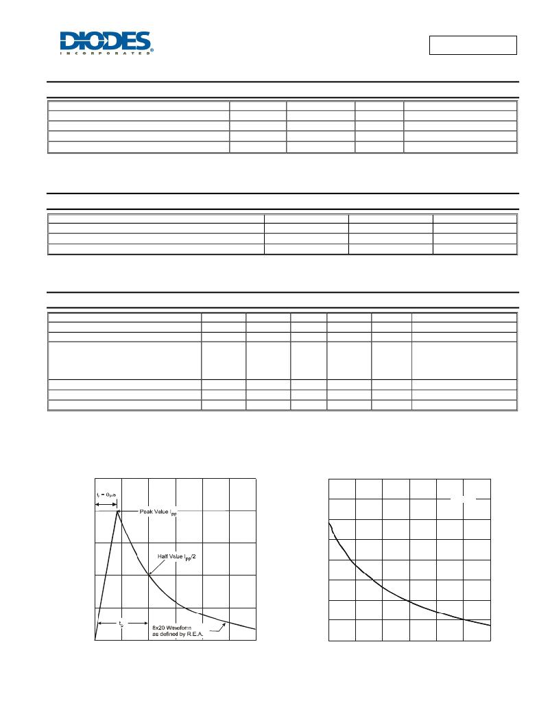
18
100
17
16
15
14
f = 1 MHz
50
13
12
11
0
0
20
40
60
10
0
1
2 3 4 5 6
t, TIME ( μ s)
Fig. 1 Pulse Waveform
V R , REVERSE VOLTAGE (V)
Fig. 2 Typical Total Capacitance vs. Reverse Voltage
D5V0L1B2LP4
Document number: DS35586 Rev. 4 - 2
2 of 4
January 2012
? Diodes Incorporated
发布紧急采购,3分钟左右您将得到回复。
相关PDF资料
D5V0L1B2T-7
TVS DIODE 5V 1CH BI SOD523
D5V0L1B2WS-7
TVS DIODE 5V 1CH BI SOD323
D5V0L2B3SO-7
TVS DIODE 5V 2CH BI SOT23
D5V0L2B3T-7
TVS DIODE 5V 2CH BI SOT523
D5V0L2B3W-7
TVS DIODE 5V 2CH BI SOT323
D5V0L4B5S-7
TVS DIODE 5V 4CH BI SOT353
D5V0L4B5SO-7
TVS DIODE 5V 4CH BI SOT25
D5V0L4B5TS-7
TVS DIODE 5V 4CH BI TSOT25
相关代理商/技术参数
D5V0L1B2LP-7B
功能描述:TVS 二极管 - 瞬态电压抑制器 1 CH TVS BI Array 5.0 Volts 84W 6A RoHS:否 制造商:Vishay Semiconductors 极性:Bidirectional 工作电压: 击穿电压:58.9 V 钳位电压:77.4 V 峰值浪涌电流:38.8 A 系列: 封装 / 箱体:DO-214AB 最小工作温度:- 55 C 最大工作温度:+ 150 C
D5V0L1B2T-7
功能描述:TVS 二极管 - 瞬态电压抑制器 BI 10.1 to 20pF 1Ch 2 Pin SOD523 TVS RoHS:否 制造商:Vishay Semiconductors 极性:Bidirectional 工作电压: 击穿电压:58.9 V 钳位电压:77.4 V 峰值浪涌电流:38.8 A 系列: 封装 / 箱体:DO-214AB 最小工作温度:- 55 C 最大工作温度:+ 150 C
D5V0L1B2TS7
制造商:DIODES 制造商全称:Diodes Incorporated 功能描述:LOW CAPACITANCE BIDIRECTIONAL TVS DIODE
D5V0L1B2TS7B
制造商:DIODES 制造商全称:Diodes Incorporated 功能描述:LOW CAPACITANCE BIDIRECTIONAL TVS DIODE
D5V0L1B2WS
制造商:DIODES 制造商全称:Diodes Incorporated 功能描述:LOW CAPACITANCE BIDIRECTIONAL TVS DIODE
D5V0L1B2WS-7
功能描述:TVS 二极管 - 瞬态电压抑制器 BI 10.1 to 20pF 1Ch 2 Pin SOD123 TVS RoHS:否 制造商:Vishay Semiconductors 极性:Bidirectional 工作电压: 击穿电压:58.9 V 钳位电压:77.4 V 峰值浪涌电流:38.8 A 系列: 封装 / 箱体:DO-214AB 最小工作温度:- 55 C 最大工作温度:+ 150 C
D5V0L1B5LP37
制造商:DIODES 制造商全称:Diodes Incorporated 功能描述:LOW CAPACITANCE BIDIRECTIONAL TVS DIODE
D5V0L1B5LP37B
制造商:DIODES 制造商全称:Diodes Incorporated 功能描述:LOW CAPACITANCE BIDIRECTIONAL TVS DIODE
